We carry and count on them nearly every minute of the day, yet few of us appreciate the immeasurable impact that transistors make every minute of our lives. Like the cells that make up our complex human bodies, their arrangement is the basis for computers, cell phones, radios, and anything else that runs on integrated circuits.
Transistors are fundamental. A transistor is a switch. But we can control it with voltage, using a small input current to turn a larger current on and off. And it can switch tens of billions of times per second. To understand them is to understand the foundation of modern devices, an apt starting point in demystifying the computer-driven world around us. Discover the secrets of these technological building blocks as we explore how transistors work and where we use them to make our lives easier.

How Does a Transistor Work?
A transistor is a simple component consisting primarily of silicon. Existing chiefly as silicon dioxide (SiO2, or silica), silicon is the second-most abundant element in the Earth’s crust. We mine over 8 million metric tons of silicon annually,1 primarily from quartz, using its semiconducting properties in computer chips and electronics.
John Bardeen, William Shockley, and Walter Brattain demonstrated the technological advantages of silicon when they invented the first transistors in the late 1940s. In electronics, transistors act as gateways on an electrical signal’s path, allowing us to amplify it and turn it on and off. As an audio and radio amplifier, it turns a weak input signal into a larger output signal. Transistors make tools like FM receivers and hearing aids possible.
We can create an integrated circuit, or microchip, by combining immense quantities of transistors. With millions strung together, there are limitless combinations of possible on and off positions. We can then put them together as logic gates, in which various combinations of binary inputs create conditional outputs. By employing Boolean logic, transistors allow computers to make numerous decisions and perform functions instantaneously.
Silicon Doping
Transistors work through electron transfer. Silicon is the backbone of the process, a semiconductor that can enable and disable electron flow with the help of a small current. By itself, electrons in silicon atoms fit neatly together and are unlikely to move. But when we introduce impurities to the silicon (aka “doping”), we can add and move electrons freely.
Doping involves adding another substance to change the number of electrons associated with the silicon. Silicon has four electrons in its outermost shell (valence electrons). A substance like phosphorus, arsenic, or antimony contains five valence electrons. When we add a phosphorus atom to a lattice of silicon, four valence electrons will match with corresponding silicon atoms, but one will float freely. Giving silicon extra free-floating electrons in this way creates an n-type (or negative-type) silicon.
When we dope the opposite way, we take electrons from the lattice. Holes open up when there is an atom that has only three valence electrons, such as a boron or aluminum atom. In other words, a boron atom’s three valence electrons would pair with three of the four surrounding silicon atoms. The fourth would have an empty spot. The hole where the missing electron would sit functions as a positive charge, giving this silicon the label “p-type.”
Both n-type and p-type silicon are neutral despite the labels, as they still have the same number of electrons and protons. But the two silicons combine in different ways within transistors to let us affect how they operate when we introduce a current.
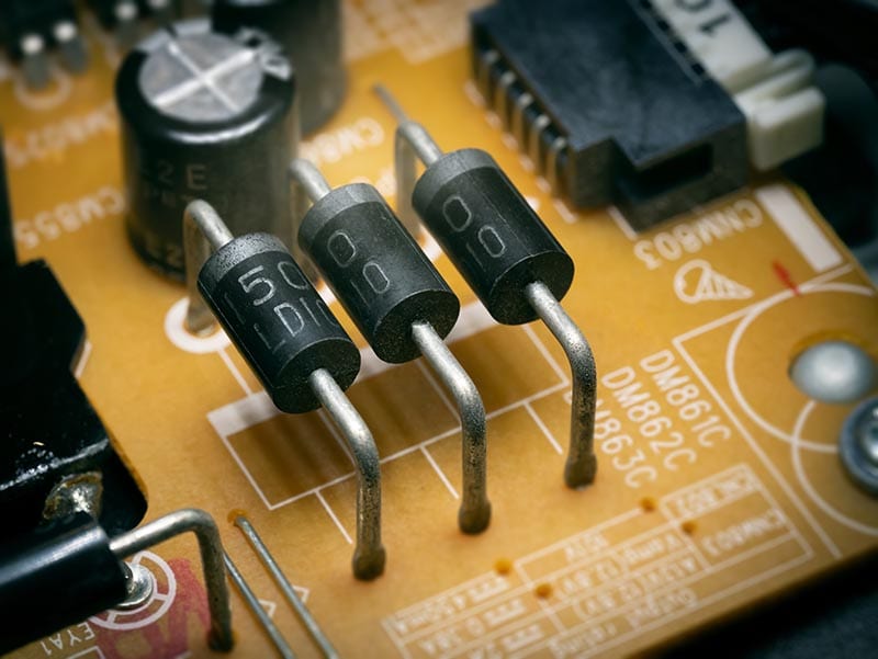
Diodes: The Transistor Precursor
To see how doped silicon in n-type and p-type forms interact in a transistor, we can start with a more basic structure—the diode. A diode puts a p-type and an n-type together. At the junction, some of the excess electrons in the n-type silicon move to fill the holes in the p-type silicon, creating a barrier where the p-type has some negative charge and the n-type has some positive charge. Electrons cannot pass this boundary, called the depletion layer, once in place, as the negative p-type forces resist further flow.
If you hook the diode up to a power source, you can overcome the resistance to electron movement. When you connect the terminals to a battery, the positive end will attract electrons. With enough power, typically at least 0.7V, the electrons will move to holes further back in the p-type layer and toward the battery. The p-type holes at the depletion layer open up, and electrons from the n-type layer can jump over. Meanwhile, the negative terminal pushes electrons into the diode toward the junction, allowing the current to flow, a process called forward biasing.
We can also hook up a battery in the opposite direction to create a reverse bias. If the positive end of a battery were to pull on the n-type’s electrons, and the negative end pulled on the positive holes in the p-type, the depletion layer would widen. Electricity cannot flow in this configuration. As a result, diodes act as one-way switches.
What Are the Different Types of Transistors?
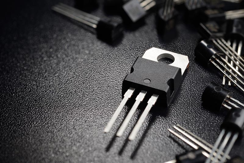
The jump from a diode to a transistor involves the addition of another n-type or p-type layer, creating two P-N junctions and depletion regions. A binary junction transistor (BJT) is a common type that uses n-type and p-type silicons in three-layered configurations. In an NPN transistor, two n-type terminals sit on either side of a p-type inner terminal. The opposite occurs in a PNP transistor.
In both transistors, the base is the center terminal sandwiched between two leads. The emitter is the negative terminal that emits the charge. The collector collects it as the positive terminal.
NPN vs. PNP Transistors
An NPN transistor features a heavily doped emitter, a doped collector, and a lightly doped base. The transistor passes electrons from the emitter through a thin base and onto the collector. The collector then sends those electrons to the next part of the circuit. The conventional current, in this case, runs from the collector to the emitter, as the positive terminal draws electrons through the collector.
In a PNP transistor, the polarities and the current reverse. While the base still controls the current, the current sinks to it from the emitter. Instead of electrons, the positively charged holes are the charge carriers in this arrangement.
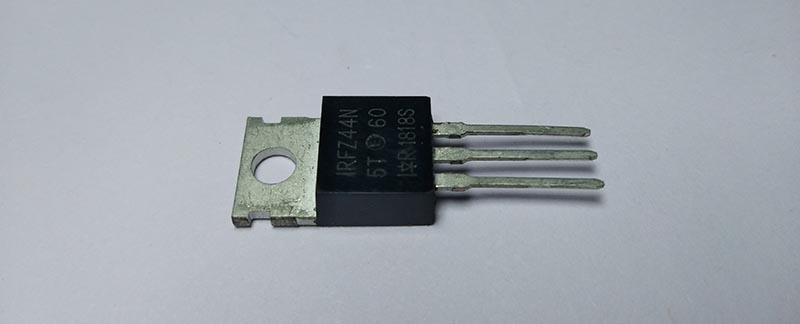
Field-Effect Transistor
To replace the BJT’s emitter, collector, and base, a field-effect transistor (FET) uses a source, drain, and gate. Though they also operate by moving electrons with n-type and p-type layers, FETs don’t linearly arrange them. Instead, a channel exists between the source and drain to allow a current to pass.
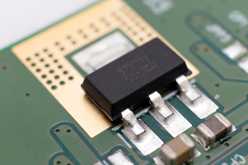
Depending on the type of FET, the current may always be on or off when no voltage is applied. By adding voltage at the gate, the channel can widen or open through a changing depletion region, allowing us to control the amount of current that can flow. The MOSFET, featuring a metal oxide layer at the gate, is one of the most common transistors you’ll find today.
Where Is It Used?
Transistors are essential components in modern electronics. As electrical amplifiers, transistors appear in hearing aids, radios, stereo systems, and countless other devices. The most common transistor uses take advantage of their switch-like features. In simple forms, you can find them around the home to relay signals and activate air conditioners, smoke alarms, and appliances.
Transistors make modern digital technology possible when we put millions or billions together. Millions of microscopic transistors merge in microprocessors, following logical operations that allow anything with a computer to run programs and perform tasks. Vast amounts of transmitters can also hold charges, using their switching ability to store data in memory cards.
Advantages of Transistors
Transistors offered numerous benefits over their vacuum tube predecessors when they first arrived in the mid-20th century. The primary difference was the immediate potential in scale. With no moving parts (save the flow of electrons), these solid-state components could be incredibly tiny. Devices could, subsequently, become smaller, lighter, longer-lasting, and far more energy-efficient.
Disadvantages of Transistors
The transistor’s size is simultaneously one of its greatest advantages and a significant drawback. Creating transistors and replacing faulty ones is a complex process and not one that someone at home can easily accomplish. And unfortunately, they’re delicate. They have a low thermal tolerance and are susceptible to breakdown from high voltage inputs.

Frequently Asked Questions (FAQs)
How Big Is a Transistor?
In 1965, Intel CEO Gordon Moore introduced the concept that transistors would continually become smaller and more capable, estimating that microchips would double their transistor capacity every 2 years. And despite more transistors, microchips will also become cheaper.
Although it hasn’t kept up exactly with Moore’s Law, transistor evolution has continued steadily, and our progress is defying expectations even for industry experts. The best microchip in the 1980s would have less than 500,000 transistors, but an average smartphone now features over one billion. The Apple iPhone 14 boasts an A16 chip with nearly 16 billion transistors running it. Today’s transistors can be as small as two nanometers, thinner than a strand of DNA.
Moore’s Law does have a limit. As we compress transistors to smaller sizes, quantum effects such as tunneling can occur, in which electrons move across the transistor independent of the gate’s input. Issues appear in transistors at under roughly 5 nm, and scientists have thus far been able to mitigate this unconventional behavior. But now, with FET gates as small as 0.34 nm, the final miniaturization of transistors is moving closer in sight.

Conclusion
Transistors are so microscopically small that they can’t help but be out of sight and out of mind for the average person. Yet nearly every modern luxury we enjoy wouldn’t exist without them. They are the DNA of technology, and as they evolve, they will dictate the direction of devices, electronics, and the world.
Featured Image Credit: Andrei Kuzmik, Shutterstock
Contents